
1. Introduction
Electrocardiograms (ECGs) measure extremely small electrical signals generated by the heart, typically on the order of a few millivolts. Accurately capturing these signals places demanding requirements on the analog-to-digital converter (ADC), which must:
- Detect very small voltage variations (high resolution)
- Reject unwanted interference (high signal-to-noise ratio)
- Accurately capture low-frequency content (ECG signals typically span 0.05–150 Hz)
Meeting these requirements requires both precision and robustness throughout the signal chain. Delta-Sigma (ΔΣ) ADCs are particularly well suited for ECG acquisition due to their high resolution, excellent noise performance at low frequencies, and inherent digital filtering capabilities.
However, fully exploiting the advantages of a ΔΣ ADC requires more than selecting the right device. A solid understanding of the modulator's operation, feedback behavior, and configuration parameters is essential to properly tune the system for real-world ECG signals. This article provides an in-depth, intuitive explanation of ΔΣ modulation and demonstrates how its key building blocks work together to achieve high-resolution, low-noise digitization.
2. ΔΣ-ADC Overview
A ΔΣ ADC consists of two main functional blocks: an oversampling ΔΣ modulator followed by a digital decimation filter. Together, these blocks convert a low-bandwidth analog signal into a high-resolution digital output.
The key idea behind ΔΣ conversion is deceptively simple yet powerful: instead of sampling just fast enough to meet the Nyquist criterion, the input signal is sampled much faster than required. This oversampling spreads the quantization noise over a wide frequency range. Through noise shaping, most of this quantization noise is pushed to higher frequencies, well outside the signal band of interest. A digital filter then removes the out-of-band noise and reduces the data rate, yielding a clean, high-resolution digital result.
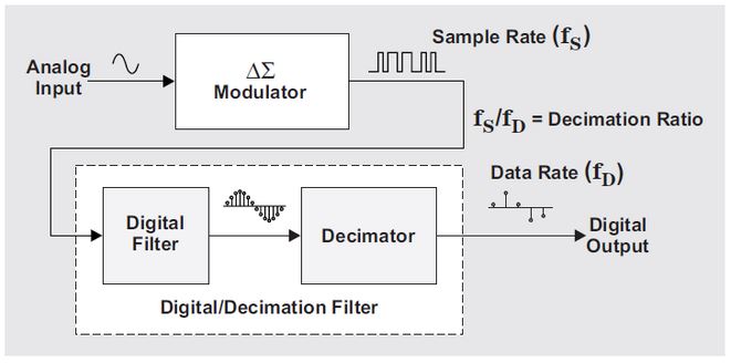
As illustrated in Figure 1, the ΔΣ modulator operates at a very high sampling frequency and converts the analog input into a coarse 1-bit data stream. While this stream has low instantaneous resolution, it accurately captures the signal information over time. The subsequent digital/decimation filter processes this high-rate bitstream, suppresses the shaped high-frequency noise, and produces a slower, multi-bit digital output with significantly improved resolution.
A ΔΣ ADC therefore operates in two stages, each running at a different speed:
- ΔΣ Modulator (fast)
Operates at the sampling frequency (fs) and generates a high-rate 1-bit output stream. - Digital / Decimation Filter (slow)
Processes the modulator output to produce the final digital code at a much lower data rate (fD), while restoring full resolution.
To demonstrate the functionality of a ΔΣ ADC, a simulation in this article is made using a 1 Hz sine-wave input. This low-frequency signal highlights the benefits of oversampling and noise shaping, making the behavior of the modulator and decimation filter easy to observe.
The simulation parameters used in this example are:
- Input amplitude: 0.9 (normalized), representing a small-signal input after front-end amplification
- Input frequency: 1 Hz, corresponding to a slow-changing signal
- Sampling frequency: 1024 Hz, resulting in an oversampling ratio (OSR) of 512 for a 1 Hz signal
- Comparator reference voltage: 0 V, centering the 1-bit quantizer
- Number of cycles: 3, allowing multiple signal periods to be visualized
- Verbose output: Disabled, focusing on signal behavior rather than internal debug data
These settings provide a clear and intuitive example of how a ΔΣ ADC converts a low-frequency analog signal into a high-resolution digital representation.
2.1 Part 1: The Modulator
The ΔΣ modulator is the core building block of a ΔΣ ADC. It converts an analog input signal into a high-rate digital bitstream while spectrally shaping the quantization noise introduced by the digitization process. Quantization noise is the error that arises because a continuous-amplitude signal must be represented using a finite set of discrete digital levels.
Throughout this article, the term noise refers specifically to this quantization noise.
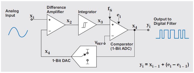
The modulator achieves this behavior using a closed-loop architecture composed of four fundamental circuit elements:
- A difference amplifier that subtracts the feedback signal from the input
- An integrator that accumulates the resulting error over time
- A comparator (1-bit quantizer) that converts the integrator output into a binary decision
- A 1-bit DAC that converts this decision back into an analog level for feedback
Rather than attempting to suppress quantization noise uniformly across all frequencies, this feedback structure enables a technique known as noise shaping. Noise is pushed away from low frequencies—where the signal of interest resides—and toward higher frequencies. Because these high-frequency components lie outside the signal band, they can later be removed using digital filtering and decimation.
The following sections examine each of these building blocks in detail and show how their interaction within the feedback loop enables high-resolution analog-to-digital conversion.
2.1.1 Modulator Stages
Having established the structure and purpose of the ΔΣ modulator, this section focuses on the operation of its individual stages.
The modulator operates at the sampling frequency fS. On each clock cycle, all four blocks—the difference amplifier, integrator, comparator, and 1-bit DAC—update once, forming a complete iteration of the feedback loop. The clock period therefore defines the sampling interval at which the input signal is processed.
To build intuitive understanding, each stage will first be examined in the time domain, emphasizing how signals evolve from one sample to the next within a single clock cycle. Rather than beginning with frequency-domain theory, the behavior of each block will be explained using simple time-domain waveforms.
After the conceptual explanation, each stage will be simulated using the input signal defined above, allowing the effect of each block on the signal and feedback path to be observed directly before considering their combined noise-shaping behavior.
2.1.1.1 Difference Amplifier
The ΔΣ modulation loop begins with the difference amplifier, which computes the instantaneous error between the input signal and the feedback signal generated by the 1-bit DAC.
At each sampling instant, the input sample Xn is compared with the DAC output X4. The resulting difference forms the error signal X2:
X2 = Xn - X4The behavior of the 1-bit DAC determines the sign of the feedback:
- When the modulator output is 1, the DAC produces +Vref, which is subtracted from the input.
- When the modulator output is 0, the DAC produces −Vref, which effectively adds Vref to the input.
In the time domain, this operation continuously forces the loop to compare the current input level against the most recent quantized estimate of that input. The resulting error signal represents how far the system's 1-bit output deviates from the true analog value at that moment.
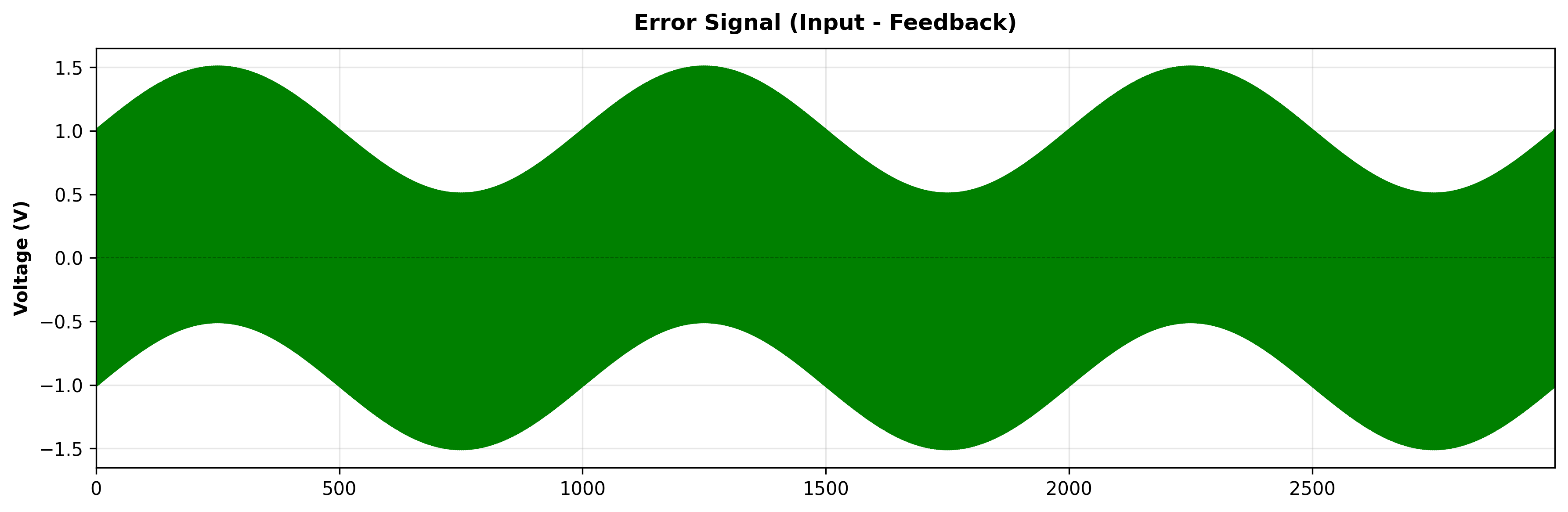
This error signal drives the remainder of the feedback loop. Without an accurate difference calculation at this stage, the integrator would accumulate incorrect information, and the modulator would be unable to compensate for quantization error or achieve effective noise shaping.
2.1.1.2 Integrator
The integrator accumulates the error signal produced by the difference amplifier and stores it over time. At each sampling instant, the current error X2[n] is added to the integrator's previous state:
X3[n] = X3[n − 1] + X2[n]This accumulation is the defining characteristic of sigma-delta modulation. Rather than responding only to the current input sample, the integrator maintains a memory of past errors. Its output therefore represents the running sum of all previous discrepancies between the input signal and the feedback signal.
The comparator uses the integrator output X3[n] to determine the next modulator output. Because the integrator retains information from earlier samples, errors at consecutive time steps become correlated. For example, if the error at one instant is large and positive, the integrator output increases, making it more likely that the next quantized output will drive the error in the opposite (negative) direction to compensate.
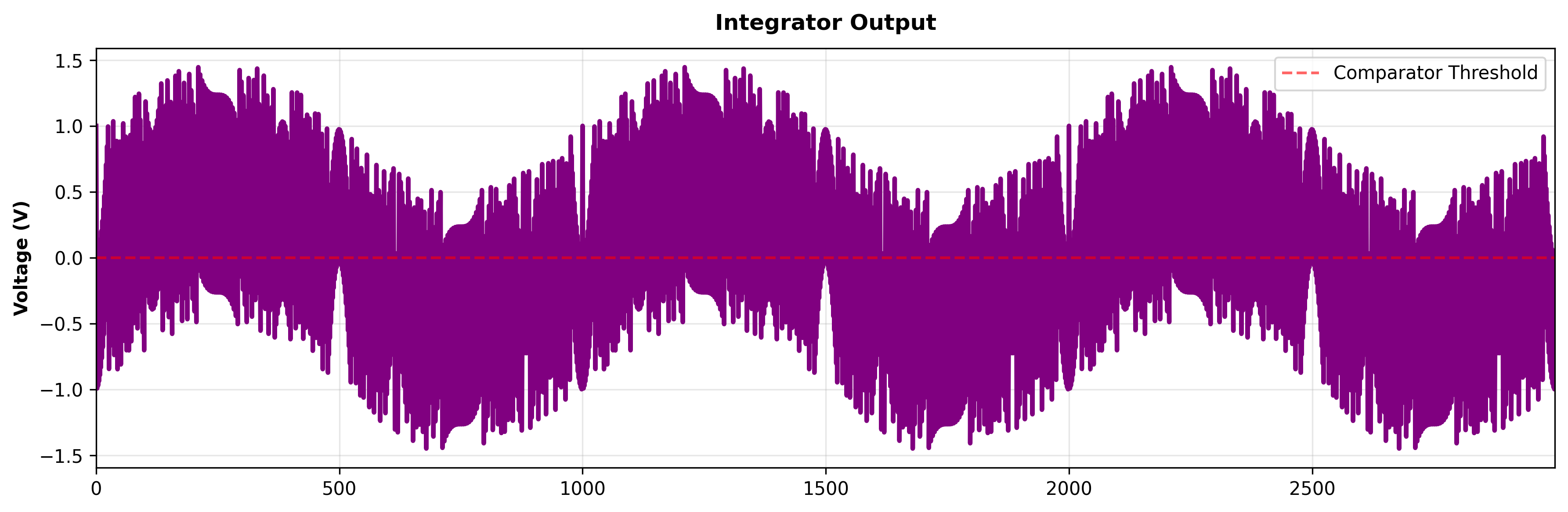
This intentional correlation transforms the quantization error from uncorrelated, flat (white) noise into shaped noise. In mathematical terms, the error sequence transitions from a simple error term e[n] to a differenced form e[n]−e[n−1]. As a result, low-frequency error components are suppressed while higher-frequency components are emphasized.
In effect, placing the integrator inside the feedback loop causes the quantization noise to experience a high-pass characteristic, which is the fundamental mechanism behind noise shaping in a first-order ΔΣ modulator.
2.1.1.3 Comparator (1-bit ADC)
The comparator converts the integrator output into a digital signal by comparing it against a reference threshold. This block is the actual analog-to-digital conversion element within the ΔΣ modulator.
At each modulator clock pulse, the comparator evaluates the integrator output and produces a 1-bit result:
- If the integrator output is greater than the reference level, the output is 1
- If the integrator output is less than the reference level, the output is 0
This binary decision is made at every sampling instant, making the comparator a 1-bit quantizer. Although each individual decision is extremely coarse, the high sampling rate and the feedback loop allow accurate signal information to be conveyed over time.
The comparator output directly determines the next feedback value generated by the 1-bit DAC. In this way, the comparator closes the loop by translating the integrator's accumulated error into the digital bitstream that represents the modulator output.
2.1.1.4 1-bit DAC (Feedback Path)
The 1-bit DAC converts the comparator's digital output back into an analog voltage, thereby closing the feedback loop. This feedback path is what transforms the modulator from a simple quantizer into a self-correcting system capable of noise shaping.
Much like pulse-density modulation (PDM), the DAC output represents an average analog value over time, even though it can assume only two discrete levels at any given instant. The DAC maps the comparator's binary output as follows:
- 1-bit output = 1 → DAC output = +VREF
- 1-bit output = 0 → DAC output = −VREF
This analog feedback signal is subtracted from the input by the difference amplifier in the next clock cycle, allowing the loop to continuously correct for quantization error.
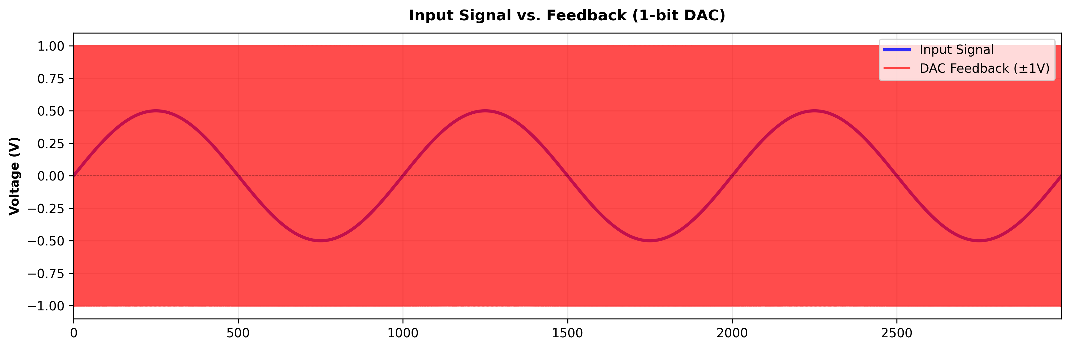
The reference voltage VREF is typically chosen to match the expected input signal range and may be ±1 V, ±2.4 V, or another application-dependent value. For proper modulator operation, the reference voltage must bracket the input signal:
|Xin| < |VREF|If the input signal exceeds ±VREF, the modulator saturates. In this condition, the feedback can no longer track the input, and the output bitstream becomes stuck at all 1s or all 0s. A common design guideline is to choose:
VREF ≈ 1.15–1.2 × Xin,maxproviding approximately 15–20% headroom to accommodate signal peaks and avoid overload.
It is important to note that the DAC switches between ±VREF, not necessarily ±1. These levels define the full-scale feedback range of the modulator and must be sufficient to cover the maximum expected input amplitude.
The 1-bit DAC is essential to ΔΣ modulation. Without this analog feedback path, there is no error correction, no accumulation of past errors, and ultimately no noise shaping.
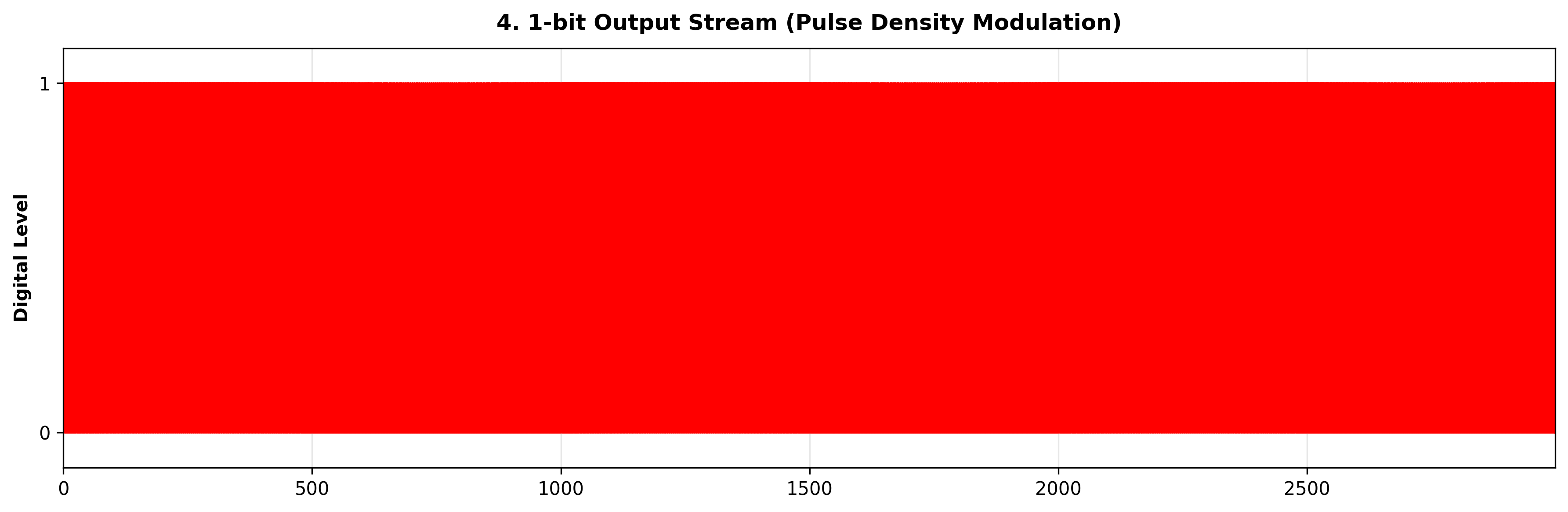
2.1.1.5 Pulse Density Modulation (PDM)
The 1-bit output of a sigma-delta modulator is best understood as pulse-density modulation (PDM). While any individual bit carries very little information on its own, the density of 1s versus 0s over many modulator clock cycles encodes the amplitude of the input signal.
When the input voltage is high, the integrator output spends more time above the comparator threshold, resulting in a higher density of 1s in the output stream. Conversely, when the input voltage is low, the integrator output spends more time below the threshold, producing a higher density of 0s. For an input near mid-scale, the integrator oscillates symmetrically around the threshold, yielding approximately equal numbers of 1s and 0s.
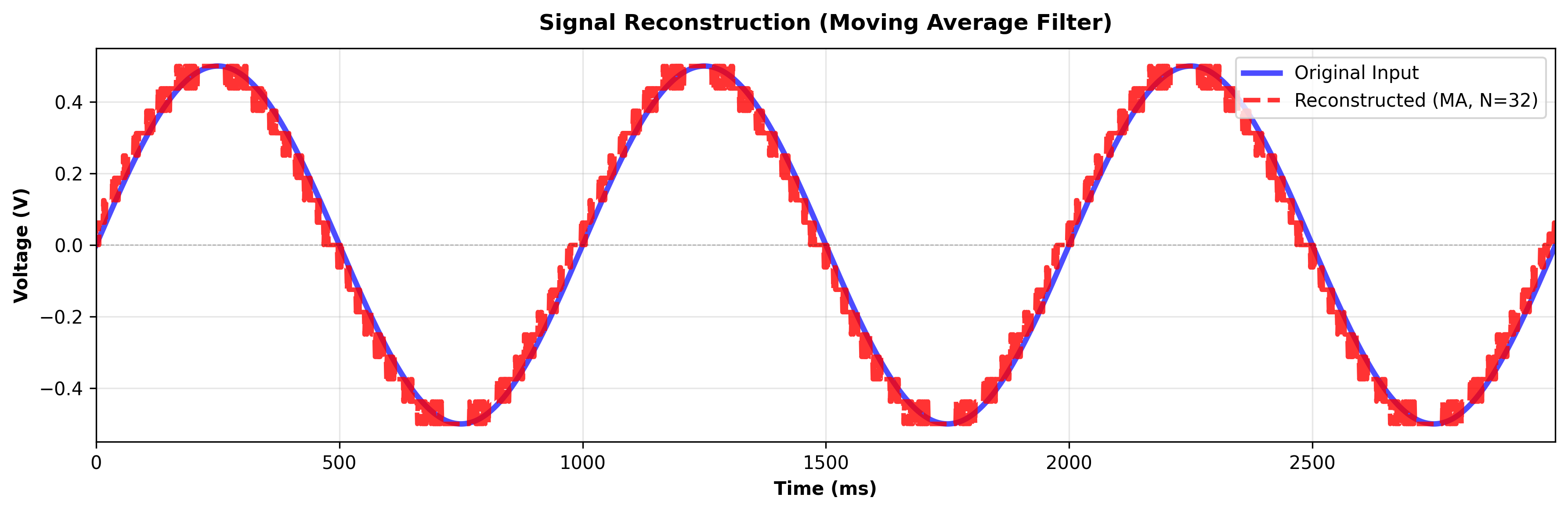
A straightforward way to interpret this PDM bitstream is to compute a moving average. If the 1-bit output is mapped to analog levels (1 → +VREF, 0 → −VREF), averaging the stream over N samples converts pulse density into a corresponding voltage level while simultaneously filtering out the high-frequency switching components.
- A higher proportion of +VREF samples produces a higher average voltage
- A higher proportion of −VREF samples produces a lower average voltage
- An equal mix averages to approximately zero
This moving average represents the simplest possible digital low-pass filter and captures the fundamental principle behind the decimation filters used in sigma-delta ADCs. Through this process, a noisy, high-rate 1-bit stream is transformed into a smooth, high-resolution digital representation of the input signal.
The output results presented in this section are generated using this principle. At each modulator clock pulse, the modulator completes a full feedback cycle and produces a new 1-bit output. As the clock continues to run, the accumulated sequence of output bits forms a pulse-density-modulated stream whose average value is proportional to the input voltage relative to the reference voltage.
2.1.2 Noise Shaping
Noise shaping is the mechanism that allows a ΔΣ modulator to achieve high resolution using only a 1-bit quantizer. Instead of removing quantization noise, the modulator redistributes it in frequency, pushing most of the noise power out of the signal band.
This behavior originates from the integrator in the feedback loop. Because the integrator accumulates past errors, the modulator actively compensates for them in subsequent samples. A positive error increases the integrator output, making a compensating negative error more likely in the next sample, and vice versa. As a result, quantization errors become correlated rather than random, preventing error energy from accumulating at low frequencies where the signal of interest resides.
In the frequency domain, this correlation transforms flat (white) quantization noise into shaped noise. For a first-order ΔΣ modulator, the noise spectrum exhibits a high-pass characteristic: low-frequency noise is strongly suppressed while higher-frequency noise is emphasized. The signal, meanwhile, remains concentrated at low frequencies.
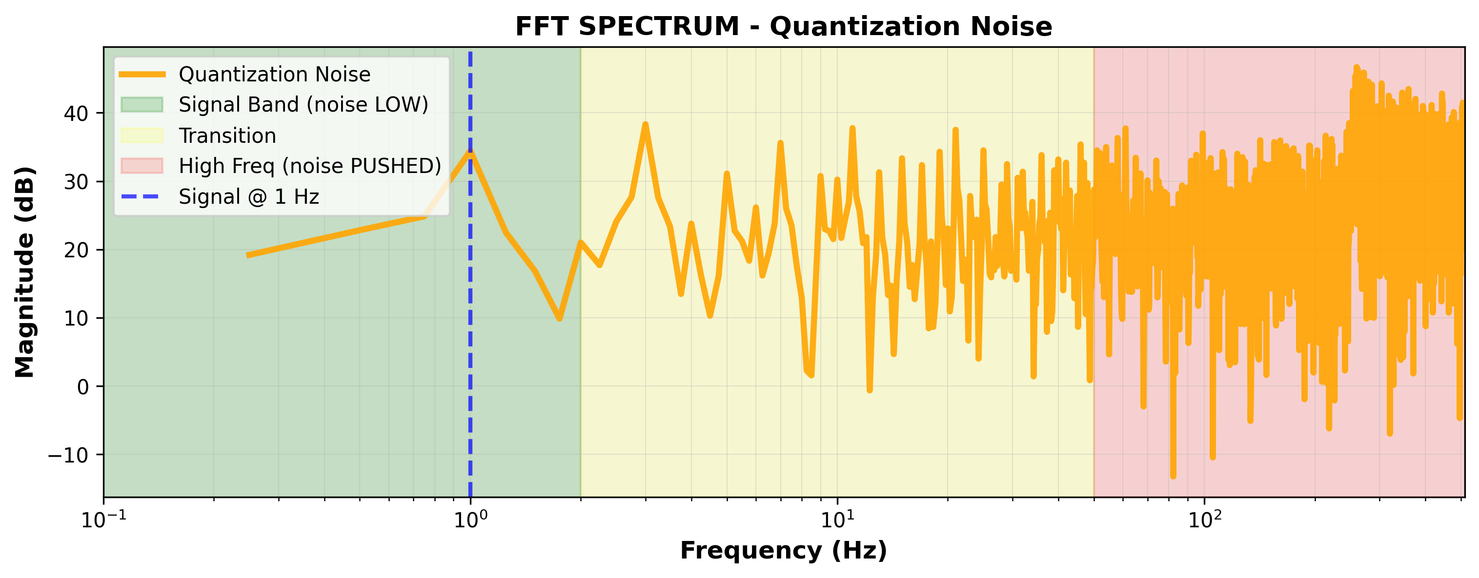
Oversampling further enhances this effect by spreading quantization noise over a wide frequency range, giving noise shaping more room to push unwanted energy out of the band. A digital low-pass (decimation) filter then removes this high-frequency noise and reduces the data rate, leaving a clean, high-resolution digital representation of the input.
In essence, noise shaping trades excess bandwidth for resolution, which is why ΔΣ ADCs are particularly well suited for low-frequency, high-precision signals such as ECGs.
Summary
Sigma-delta ADCs achieve high resolution through a brilliant strategy: accept huge quantization errors but use feedback to shape where those errors appear in frequency.
The feedback loop is the heart of the system. Without it, a 1-bit quantizer would produce terrible results—random noise spread across all frequencies. But the integrator in the feedback path creates memory of past errors, forcing consecutive errors to correct for each other. This correlation between errors manifests mathematically as the (ei - ei-1) term—a high-pass filter that pushes noise away from DC toward high frequencies.
The feedback mechanism IS a filter—it doesn't need a separate filter component. The integrator + feedback loop mathematically creates a high-pass filter on the quantization error. The digital filter at the output then applies a complementary low-pass filter, removing the shaped high-frequency noise and leaving a clean, high-resolution output.
For ECG applications, this architecture is ideal because ECG signals are low-frequency (0.05-150 Hz)—exactly where feedback-based noise shaping makes the noise floor extremely quiet. The ADS1293 demonstrates how these principles translate to practice: a higher-order modulator with multiple integrators creates steep noise shaping, while a programmable three-stage SINC filter chain allows designers to tune the balance between resolution, speed, and power consumption.